Beyond the limits of diffraction: diffractive nanostructures – Kevin Heggarty, Télécom Bretagne

They are only a few square centimeters in size and generally pass unnoticed, yet we come into contact with them every day. Diffractive optical technology is behind the holograms on our bank cards, the components which allow for uniform backlighting on certain mobile phones, and even the spinning disks which generate the grid of red light that scans the bar codes of products at the supermarket checkout. These components are a research subject at IMT, and particularly at Télécom Bretagne, where Kevin Heggarty is a lecturer and researcher in the Optics department.
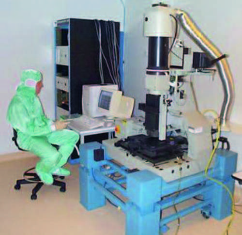
In the clean room with the photoplotter
The convergence between optical technologies and digital communication techniques continues to gather pace, optical networks, 3D displays and silicon photonics are developing more rapidly than ever before. Kevin Heggarty, now Professor in the Optics Department at Télécom Bretagne was among the first scientists to work with diffractive optical elements (DOEs)
He used DOEs, along with spatial light modulators (the micro-screen technology behind video-projectors), in the project which earned him his PhD in 1991, and they are still at the heart of his research work.
Kevin Heggarty joined Télécom Bretagne as a research engineer in 1992, focusing initially on optical neural networks. He helped design the clean room which was inaugurated in 1994, providing engineers with a new facility for design and inexpensive fabrication of DOEs.
“Businesses producing these components do so in very large numbers, churning out millions of units. DOEs are usually etched onto glass plaques, creating microstructures designed to diffract the light into a desired pattern,” Kevin Heggarty explains. A master is produced on a nickel plate, taken from the original design sculpted in photoresist. This master copy is then used to produce the DOEs in large batches. “These masters are created pixel-by-pixel,” Prof. Heggarty explains, “which can require dozens of hours’ work for a unit which measures just 5cm x 5cm. The process can cost tens of thousands of Euros.” Of course the millions of units then produced are much less expensive.
Kevin Heggarty’s innovation was to create a photoplotter based around a liquid crystal spatial light modulator. “This allows us to write an area of 1cm², using 1000 x 1000 pixels flashes, in under a minute, which means we can create prototypes and small batches at reasonable prices.” The process involves an illuminated LCD screen, with liquid crystal patterns programmed to create the micro-etched components.
Research with commercial potential
The CEA, the Meudon Observatory, the University of Michigan and almost forty other organizations have expressed an interest in this technology. “We felt that the demand was there for this small-batch technology, and a market study has confirmed that,” says Kevin Heggarty. The project continues to expand through the start-up Holotetrix (see inset) aimed at the prototype market: “We are now working with the third generation of this machine, and we have also invented a separate unit for non-visible wavelengths, while maintaining the key commercial asset of high-speed operation.”
New bridges to cross
Over the years this research has led to the publication of numerous scientific articles on the algorithms used to calculate the diffraction processes, and has provided the teams working at Télécom Bretagne with a comprehensive resource: from modeling calculations to small-batch production, via fabrication, characterisation (testing components to check that they perform as required) and prototype creation. These facilities are also used to produce components for other research teams working on optical telecommunications at Télécom Bretagne – optical micro-components are used to guide optical signals. It is now, at last, possible to replicate components without using the nickel master, producing copies on different materials: glass, silicon, printed circuits, even flexible substrates such as transparent plastic films, used to create the holograms featured on our passports.
The next challenge is to move beyond the boundaries of diffraction, though remaining in the realm of visible light. At these wavelengths, the principles of diffraction mean that etched patterns can be no smaller than 500 nanometers across. An internal research project at IMT, run jointly with partner institutions Télécom Physique Strasbourg and Télécom Saint-Étienne, hopes to reduce this minimum size to between 100 and 200 nanometers by using femtosecond lasers.
The smaller these micro-structures become, the more interest we attract from the micro-electronics sector, where such small scales are the norm.
Hololetrix, a Télécom Bretagne spin-off founded in 2007
This young company pools the expertise of its three founders (Denis Batarel, Kevin Heggarty and Jean-Louis de Bougrenet) to help clients develop new products using diffractive optical technology. Hololetrix has conducted research and produced prototypes for companies in the aerospace, automobile, chemical and packaging sectors.
Find our more: www.hololetrix.com
Born in Zimbabwe, Kevin Heggarty grew up in Scotland and studied at Cambridge
After completing his undergraduate studies in Cambridge, in 1988 Kevin embarked upon a Master of Science degree which included a six-month spell at Télécom Paris. Supported by an EU research scholarship, he wrote his PhD on the optical implantation of neural networks at a time when the potential for using optical technology to process information was just beginning to be understood.
A member of the Société Française d’Optique and the European Optical Society, he became a research director in 2010. When asked what attracted him to optical research, Kevin answers without hesitation: firstly, a longstanding interest in all things visual, secondly an influential professor who encouraged him, and finally an early intuition that optics would play an important role in the future of information processing. This intuition is now being fully borne out in today’s technological advances, with the arrival of Fibre to the Home (FTTH) and optical communication between chips, which should become a reality in 2013-2014.

